15 Jan 2020
Nano-scale X-ray vision: probing crystal defects
Coherent X-ray microscopy enables nanoscale examination of material defects and the distortions they cause, and promises new insights for the optimisation of high performance materials for aerospace and power generation.
Atoms in most metals and alloys are arranged in a regular pattern. Imperfections in this crystal structure have a dramatic effect on the properties of the material. New research at the University of Oxford allows the nano-scale examination of these defects and the distortions they cause in the surrounding material.
Felix Hofmann, Associate Professor in Oxford’s Department of Engineering Science and lead author on the study, explains: “Detailed knowledge of the structure of crystal defects is essential for optimising material performance. Normally you think of defects as being bad, however there is a fantastic opportunity here to enhance material properties by defect engineering.”
He adds: “The key element is being able to probe the distortions defects’ cause in the surrounding material, because it is through their distortions that defects communicate and interact.”
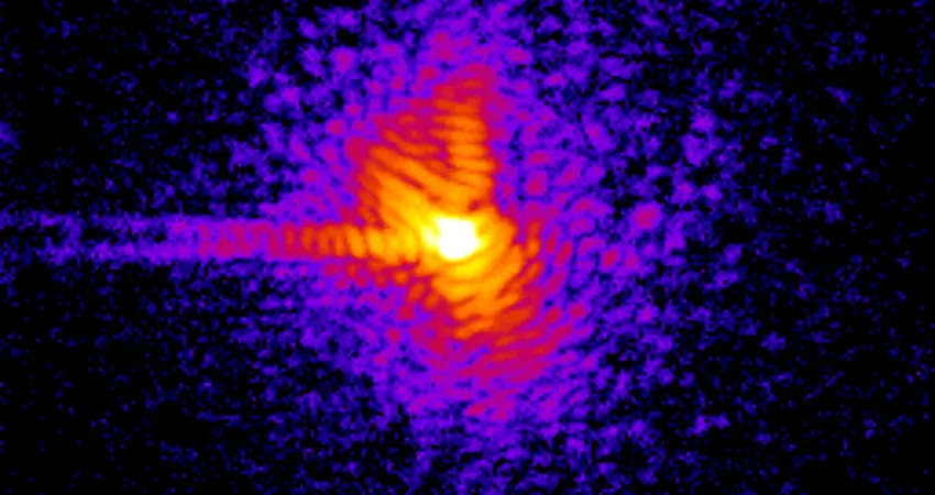
The new research, carried out in collaboration with colleagues at the Advanced Photon Source in the US, uses an X-ray diffraction technique called Bragg Coherent Diffraction Imaging (BCDI). Like a medical X-ray, BCDI allows the 3D imaging of defects, but with more than ten thousand times higher resolution. However, BCDI doesn’t just “see” the defects, but it can measure the distortions they cause in the surrounding material. Dr Nick Phillips, second author on the study and a Postdoctoral Research Associate at Oxford’s Engineering Science Department, explains: “Our new analysis approach allows us to completely characterise the lattice distortions defects cause. Importantly our method is completely general, so we can be sure it will work no matter what defects our samples contain. This is a real breakthrough in the field.”
To work, BCDI requires very small samples – less than a micron in diameter. In the past this has meant that it could only be used to investigate materials that naturally form suitably small particles. Unfortunately, almost none of the most important engineering materials fall into this category. Another problem is that it’s not until researchers examine their nano-sized samples that they know whether they in fact contain the defect they’re trying to study or not.
Lattice defects video
Watch a video of the new technique in action
Professor Hofmann’s team developed a new approach that overcomes these hurdles. It makes it possible to first identify specific defects of interest in a bulk specimen, and to then create a micron-sized BCDI sample containing these defects. This is done using an approach called Focused Ion Beam Machining (FIB) that uses a beam of focussed ions to cut and shape materials with nano-scale precision. However, FIB has its drawbacks: “BCDI has excellent sensitivity to lattice strain,” Dr Phillips elaborates, “and the presence of FIB damage causes severe complications. Even a single FIB imaging scan can leave behind large strain fields that complicate BCDI reconstructions and can obscure more subtle strain fields of interest. The key aspect of our new FIB preparation method of BCDI samples is that it provides a reliable approach for minimising FIB damage and associated spurious lattice strain fields.”
"This technique has the potential to change our understanding of the advanced alloys used in industries such as aerospace and nuclear power"
“Together, these new capabilities open the door to BCDI as a microscopy tool for studying complex real-world materials.”
In the paper, the team demonstrate the effectiveness of their new technique on tungsten, the most promising material for armour components in future nuclear fusion rectors. In service, tungsten armour will be exposed to intense heat and radiation levels for tens of years. This extreme environment causes defects within the metal, and it’s vital for engineers to understand how those defects might impact the material’s strength – particularly in the event of an accident.
Professor Hofmann adds: “We’re very excited to publish this ground-breaking research. It’s the culmination of a nine year ambition, and a lot of work has gone into it. This technique has the potential to change our understanding of the advanced alloys used in industries such as aerospace and nuclear power. We really want to get it out there as an enabling tool for the research community.”
Find out more about the work of the Solid Mechanics and Materials Group


